
I/O to FPGAs over PCIE
TL;DR
If you want to deploy some logic to a FPGA and talk to that logic over PCIE, it’s harder than it has any right to be, but it can be done by gluing together Xilinx’s XDMA core and the logic using AXI. We’ll use memory mapped I/O (MMIO) to actually transfer data from the host to the FPGA.
Disclaimer
Since so much of the tooling around FPGAs is proprietary (and thus brittle as hell) so it’s worth mentioning that I got this to work using 2021.1 Xilinx tools and on an Artix 7 (PicoEVB with XC7A50T-CSG325-1).
Acronyms
One of the most annoying things about working with FPGAs is the immense number of acronyms that documentation expects you to be familiar with. Hopefully this alleviates some of your frutration with that.
- FPGA: Field Programmable Gate Array; the device which we’re programming.
- CPU: Central Processing Unit; the processor on the host device.
- I/O: Input/Output; self-explanatory.
- PCIE: Peripheral Component Interconnect (Express); the communication interface we’re using to communicate with the host device (i.e., the CPU and operating system and memory).
- AXI: Advanced eXtensible Interface; the communication interface that the components will use to communicate amongst themselves, on the FPGA itself.
- DMA: Direct Memory Access; a system that lets individual components access memory directly, independently of the CPU.
- MMIO: Memory-Mapped I/O; uses the same address space to address both memory and I/O devices. The memory and registers of the I/O devices are mapped to (associated with) address values (in the address range assigned by the DMA controller).
- IP: Intellectual Property; wacky name for a module/chunk of logic.
- RTL: Register-Transfer Level; circuits designed in terms signals and registers.
- HLS: High-Level Synthesis; a technique for translating procedural code (e.g., C++) to RTL designs.
The Kernel
As the kernel we’ll use something simple, in particular something we can use Vitis HLS to synthesize for us:
void kernel(int* out, int in){
	*out = 2*in;
}
Note that we need AXI connections to this kernel, so why not let Vitis synthesize those too (maybe I’ll add a section that implements this part too…):
void kernel(int* out, int in){
	#pragma HLS INTERFACE mode=s_axilite bundle=kernel_io port=out
	#pragma HLS INTERFACE mode=s_axilite bundle=kernel_io port=in
	#pragma HLS INTERFACE mode=s_axilite bundle=kernel_io port=return
	*out = 2*in;
}
The meanings of the syntax can be found here. Note that Vitis HLS will automatically determine if the arguments are inputs or outputs based on how they are used in the code. Note also that the interface with port=return is optional but allows us to use a control register to start and stop the IP (and auto-start), and check if the IP is “done” (has completed).
After synthesis you should get a synthesis report that looks like this:
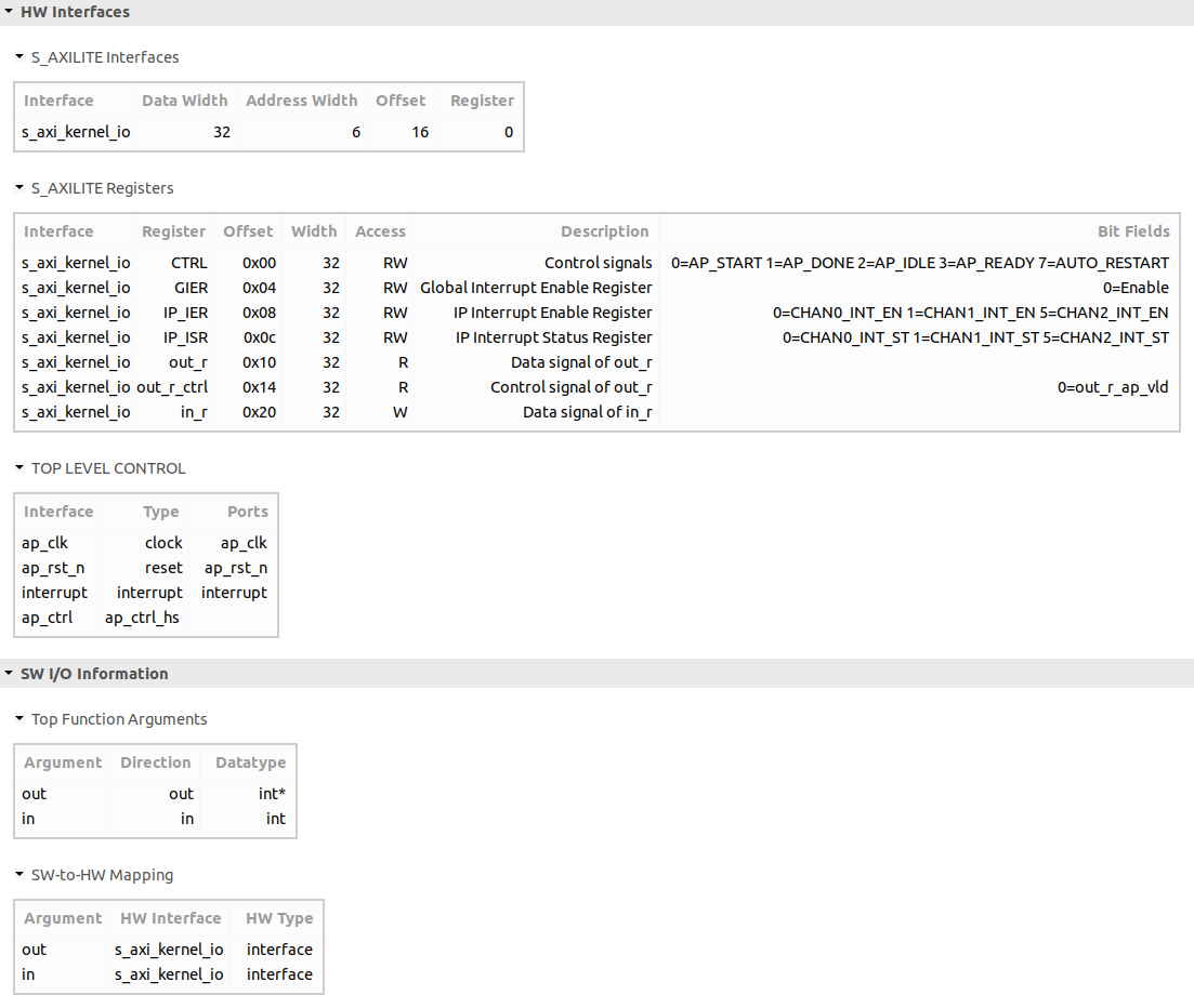
Note the CTRL, out_r, and in_r registers under S_AXILITE Registers; they’ll be important at the end (lalso, btw, S_* means streaming).
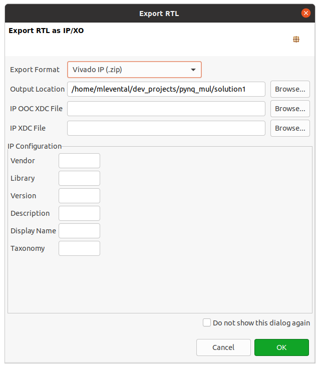
Export the RTL so that we can import it into Vivado:
Vivado
I started with the example PicoEVB project, which looks like this (under Block Design):
You can ignore most of it, but find the axi_interconnect_0 module (center here) and double click it to. Then increase the number of Master Interfaces to 5:
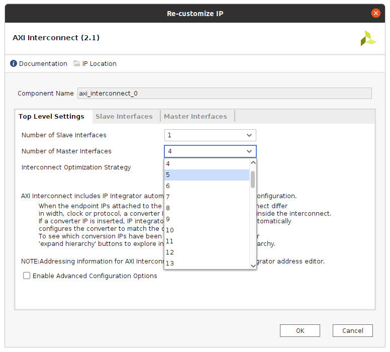
This is the interface over which we’ll be communicating with the kernel IP. Note this will add M04_AXI, M04_ACLK ,M04_ARESETN ports to the interconnect; connect the clock and reset signals to the axi_aclk and axi_resetn signals on the xdma IP core (we’ll connect M04_AXI after we add the kernel IP).
To add the kernel IP Go to IP Catalog and right click somewhere to Add Repository:
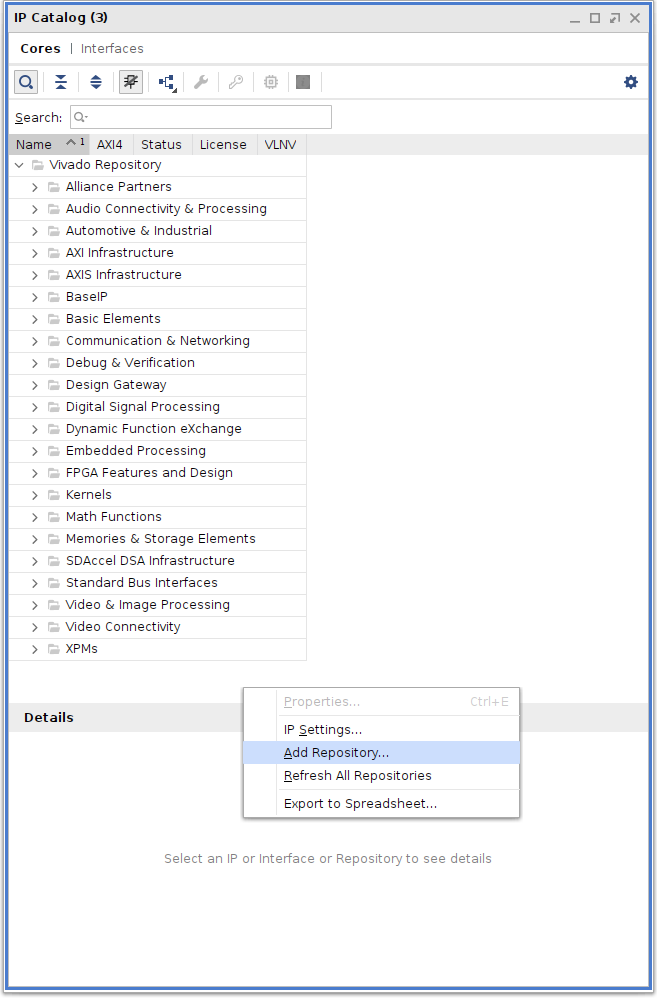
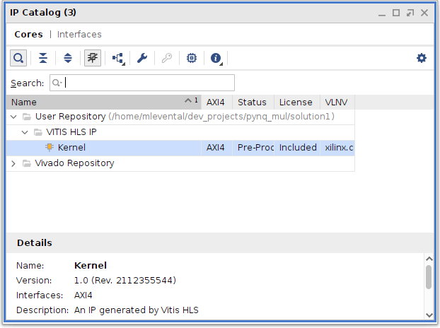
Then go through the modals and once you have User Repository in the list unfold all the tree and double click Kernel:
which adds a module that looks like this to your block design:
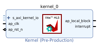
Note: don’t hit Run Connection Automation because it’ll make the wrong connections. You need to connect the s_axi_kernel_io. ap_clk, and ap_rst_n (maybe other connections need to be made but I didn’t 🤷):
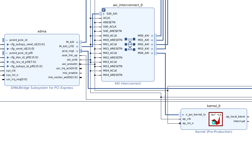
s_axi_kernel_ioconnects toM04_AXIonaxi_interconnect_0ap_clkconnects to the commonaxi_aclkclock signalap_rst_nconnects to the commonaxi_aresetnsignal
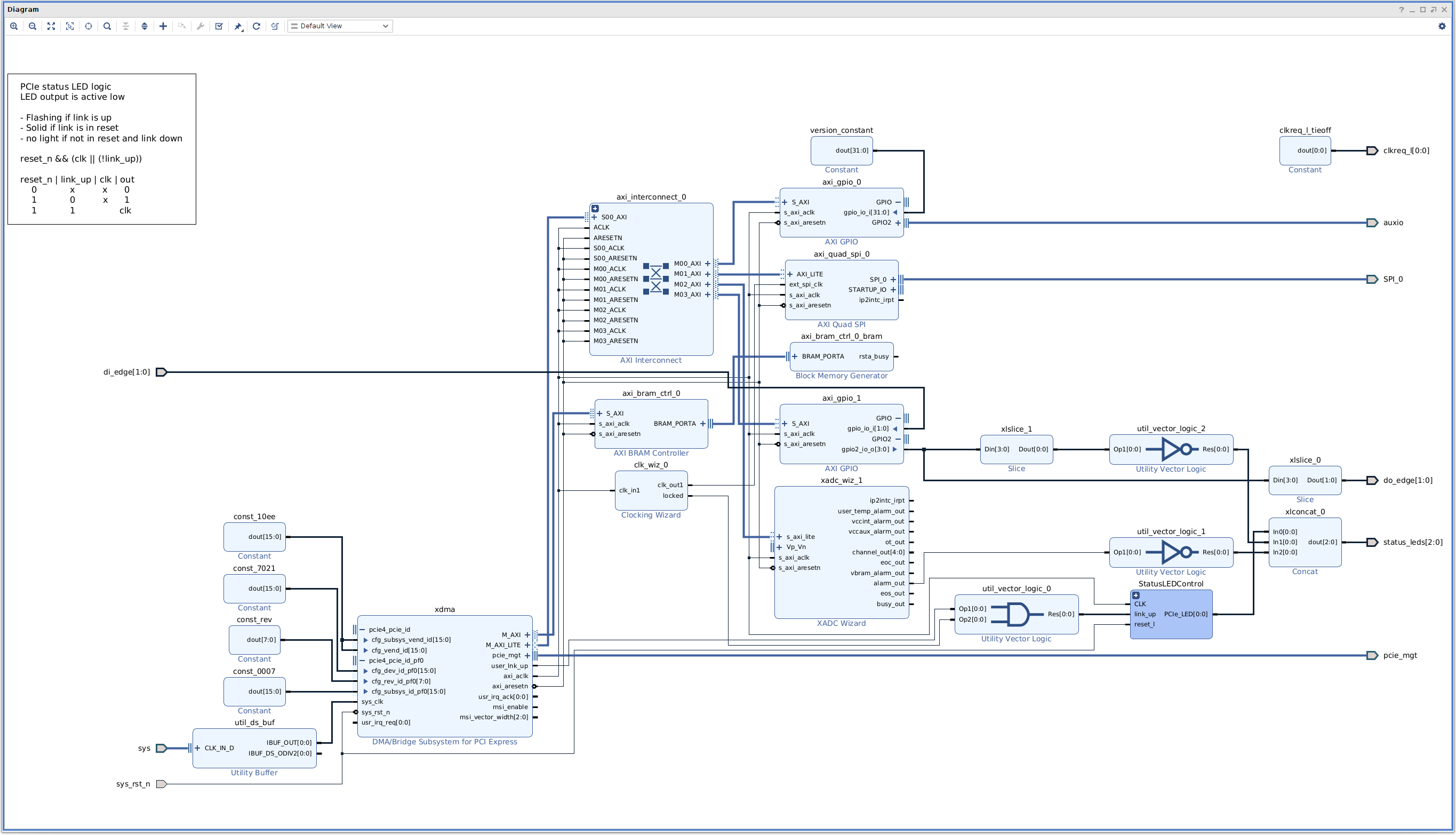
There’s lot of visual noise but your block design should look something like this after you’ve made all of the connectio
You’re probably going to need to assign the s_axi_kernel_io interface to an address space:
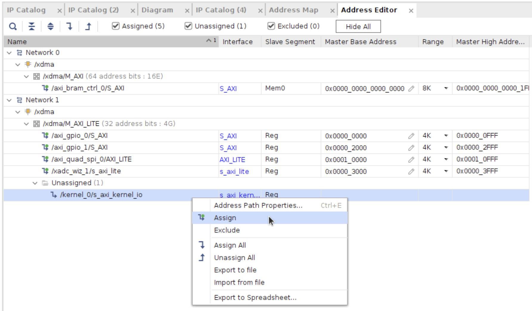
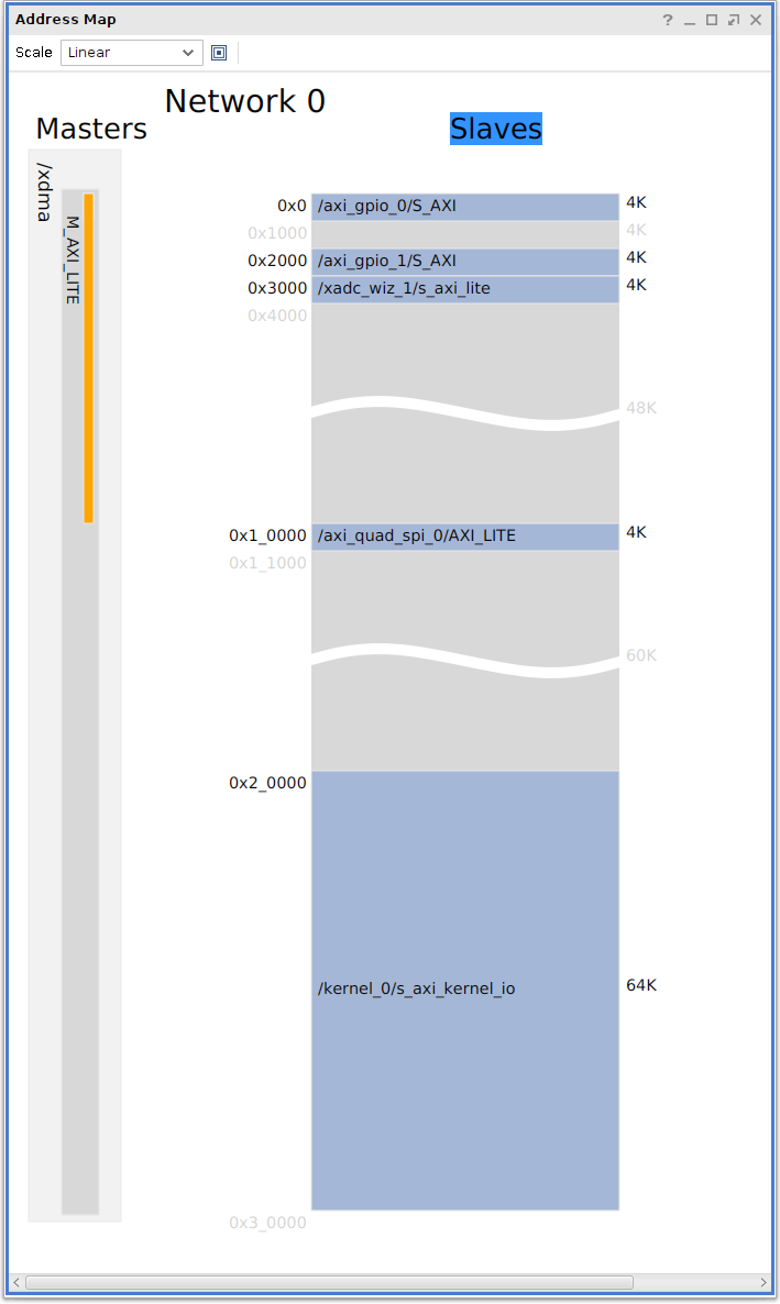
Inspecting under Address Map you can get a sense for what XDMA is really doing (i.e., mapping “master” address space to a bunch of separate “slave” address spaces):
Once all that’s done click Generate Block Design to synthesize all of the RTL. 🤞 you didn’t get any wires crossed. The click Run Implementation; fully implemented design on my part looks like this:
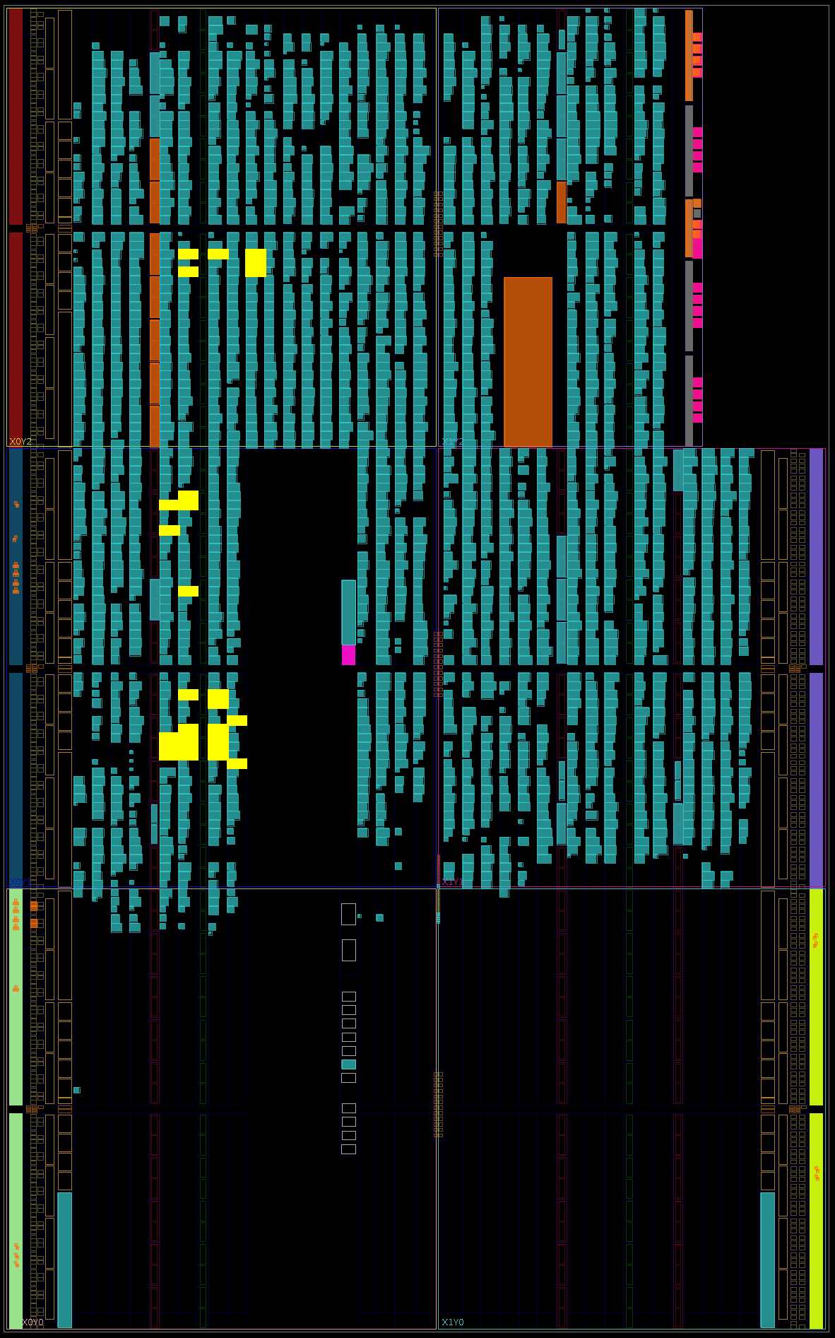
Note that the yellow scattered across the top-left is the logic for the kernel while the rest is for XDMA.
Flashing
I’m not going to into this (here is another post describing it in painful detail) but basically generate your bitstream (along with configuration memory file), connect your board, and flash.
Talking
Once you’ve flashed your board and your ready to talk to it, make sure Xilinx’s XDMA driver is loaded (see here in the post on how to get a Hello World going). Once, everything is loaded you can use this script to communicate. The actual communication is captured by
IP_BASE_ADDR = 0x0002_0000
ADDR_RANGE = 0x10000 # 65536
IN_R_OFFSET = 0x20
OUT_R_OFFSET = 0x10
CTRL_OFFSET = 0x00

def main():
  kernel_ip = MMIO(IP_BASE_ADDR, ADDR_RANGE)
  inp = 5  # number we want to double
  kernel_ip.write(IN_R_OFFSET, inp)  # write input value to input address in fabric
  print("input:", kernel_ip.read(IN_R_OFFSET))  # confirm that our value was written correctly to the fabric

  kernel_ip.write(CTRL_OFFSET, 1)  # set ap_start to 1 which initiates the process we wrote to the fabric

  outp = kernel_ip.read(OUT_R_OFFSET)
	print("output:", outp)  # read corresponding output value from the output address of the fabric
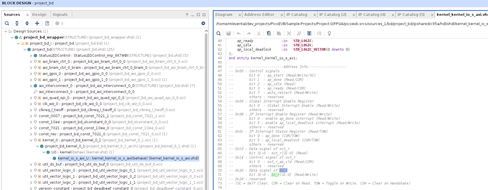
Note that the magic numbers (i.e., offsets) come from the report generated by Vitis (here) or in the synthesize RTL (not sure why this was synthesized as vhdl instead of verilog):
Assuming you did everything right you should get something like

but god speed if you didn’t 😂.